

技术线上论坛 | 5月28日《创新 | 原位AFM & SEM联用系统在表征导电和磁性纳米结构中的新应用》
发布日期:2020-05-22
Characterization of conductive and magnetic nanostructures by Correlative In-Situ AFM & SEM
创新 | 原位AFM & SEM联用系统在表征导电和磁性纳米结构中的新应用
[报告简介]
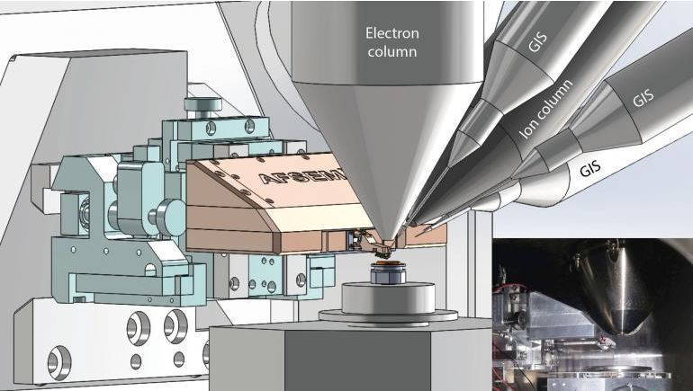
The combination of different analytical methods into one instrument is of great importance for the simultaneous acquisition of complementary information. Especially highly localized probing of mechanical, electrical, magnetic, chemical and crystallographic properties on the nanoscale represents a key success factor for gaining new insights in the micro and nano world.In this webinar, we present a unique AFM – the AFSEM – designed for seamless integration into scanning electron microscopes (SEM) or dual beam systems. It allows direct in-situ combination of these complementary techniques due to the simultaneous operation of SEM and AFM inside the vacuum chamber. Therefore, SEM imaging, chemical or crystallographic information by EDX and EBSD, real 3D topography, phase information, mechanical, electrical, magnetic and thermal properties by AFM can be combined in an easy and interactive way. Furthermore, due to the open design it can be combined with additional add-ons, e.g., tensile stages, nano-indentors or nano-manipulators. As examples for the broad variety of applications in material characterization, we will demonstrate in-situ electrical and magnetic characterization of nanostructures by combining SEM and AFM measurements.
将不同的分析表征方法集成到一种仪器设备中,实现同时获取材料或样品的多种信息,对于材料分析具有非常重要意义,也是近些年表征分析设备的重要发展趋势。特别是,在纳米尺度上对目标样品进行机械、电学、磁学、化学和晶体学性质的高度局域化探测,成为了微观和纳米世界中探究各种新现象的重要手段。
在这次网络研讨会上,来自GETec Microscopy公司的Chris Schwalb博士,将向大家展示一种独特的多功能AFM技术——AFSEM,它是一种与扫描电子显微镜(SEM)或双束系统进行集成并联用的AFM表征方案。其独特的设计理念以及工作原理,使得AFSEM可以轻松的集成到SEM腔体中,并与SEM同时进行观测,实现诸多互补表征技术的联用。它的使用并不会妨碍SEM中EBSD、EDX等表征手段的正常进行。科学家在进行交互操作的同时,便捷地对目标样品进行成像,探测其化学或晶体学信息,并对样品的三维形貌、物相信息、力学、电学、磁学和热学等性质进行测量。此外,用户友好的设计理念使得AFSEM可以与其他SEM或双束系统的常用插件和配件联用,如拉伸台、纳米压痕仪或纳米操纵器等。
作为材料表征中的经典案例,在此次报告Chris H. Schwalb博士结合多个动态视频以及来自实验室和高校的研究结果,将向大家展示SEM与原位AFSEM联用的技术优势和特点,并介绍其在纳米结构电学与磁学表征中的新前沿应用。
[注册报名]

点击https://live.vhall.com/524285102进入注册报名页面
[主讲人介绍]
Dr. Chris Schwalb
Christian H. Schwalb 博士
Dr. Christian H. Schwalb is the COO at GETec Microscopy GmbH in Vienna, where he leads the further development of the AFSEM® system – an in-situ AFM for integration into SEM and dual-beam systems. He did his PhD in the group of Prof. Ulrich Hoefer in Marburg studying charge transfer processes at metal-organic interfaces. Before joining GETec he developed a novel 3D nano-printing technique for highly miniaturized cantilever-based sensor systems in the group of Prof. Michael Huth in Frankfurt.
Christian H. Schwalb博士是奥地利维也纳GETec Microscopy有限公司的运营官,目前领导AFSEM®系统的进一步开发。AFSEM®系统是一种用于集成到扫描电镜和双束系统中的原位AFM方案。Christian H. Schwalb博士在马尔堡的Ulrich Hoefer教授组攻读博士学位,研究方向为金属-有机界面的电荷转移过程。在加入GETec Microscopy有限公司之前,他在法兰克福的Michael Huth教授团队中进行研究,研究方向为新型3D纳米打印技术在基于高度小型化悬臂梁的传感器系统上的应用。
[报告时间]
开始 2020年05月28日 14:00
结束 2020年05月28日 15:00
[直播好礼]
看直播赢好礼,更多大奖:蓝牙运动手环、智能测温水杯、多功能数据线... ...
[技术线上论坛]
http://www.qd-china.com/zh/n/2004111065734

